
Nanotechnology open house brings together researchers from across campus
The Materials Characterization Facility in the Colorado Shared Instrumentation in Nanofabrication and Characterization (COSINC) successfully hosted a focused ion beam (FIB) event in mid-April.
The FIB technique is a 'nano’ technology with several scientific and technology applications in areas ranging from materials science, to semiconductors, to the biological fields. As we know it, nanotechnology is the meeting ground of engineering, biology, physics, medicine and chemistry as most of these disciplines converge at the nanoscale, towards the same building blocks, principles and tools of investigation.
This fact was demonstrated at the open house when 40 participants from various academic departments and colleges at CU Boulder, as well as students from other local universities and companies, attended this event. The event included talks followed by a hands-on demonstration with all participants in the quiet basement of the Gallogly Discovery Learning Center, where the COSINC-CHR (Characterization) Facility is currently located.
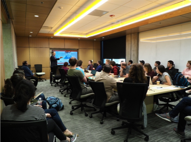
Talks at the open house, with about 40 participants from diverse academic departments from CU Boulder

Participants receiving hands-on time and demonstration on the instrument

Nano-machining on a silicon chip using the FIB instrument
“How does a FIB tool work and what are its applications?” was the question addressed by speaker Rick Passey (from FIB tool vendor, Thermo Fisher). COSINC-CHR owns several scanning electron microscopes (SEMs), which make it possible to observe micro/nano-scale objects, too small to see with optical microscopes. However, electrons are not the only charged particles that can be accelerated and focused by electromagnetic fields. A FIB instrument is almost identical to an SEM, but with an ion source instead of an electron gun. Typically, gallium ions are used and are approximately 100,000 times heavier than electrons. In addition to imaging, those heavy ions can perform “nano-machining” as the beam size can be as small as 10 nm, which is about 10,000 smaller than the size of human hair.
The FIB technique may also be used to deposit materials. One of the common applications of this technique is to prepare samples for transmission electron microscopy (TEM), by slicing samples to thicknesses of 100 nm or less. The second talk was about how an FIB instrument can be utilized in a scientific research project. A research group led by Professor Tom Perkins (JILA/MCDB) has been using the FIB instrument in the COSINC-CHR to modify tips of atomic force microscopes so that they can study the nanometer-scale dynamics and energetics of biomolecules such as DNA, RNA and proteins. Devin Edwards, a postdoctoral fellow in the Perkins group, shared his unique experience using this tool and demonstrated the improved results with their tailor-made AFM tips.
[video:https://youtu.be/92hZyZnu4JQ]
In the second half of the open house, the participants were divided into several groups for the demo sessions, where they learned about the instrument by receiving some hands-on time on the tool. Participants were excited to receive a personalized silicon chip with the Buffs logo and their initials 'engraved' on it using the ion beam.
There is a need to train the next generation of scientists and engineers in the area of nano-characterization and nano-machining, which have applications in diverse fields. This open house aimed at educating participants in this area, which may also help foster interdisciplinary research and training within the CU Boulder community.