
STED-Inspired Super Resolution Lithography
The integrated circuits in your computer or car require manufacturing processes capable of patterning billions of nanometer-scale features every second with near perfect accuracy. Moore's Law, the 50-year trend of continually smaller structures resulting in continually more powerful electronics, is possibly nearing its end. The challenge faced by the semiconductor industry is that current photolithography tools are constrained to transfer patterns with feature sizes larger than the "diffraction limit" which is roughly one half of the wavelength of the light used to project the pattern. Although the industry is exploring a new generation of tools using extreme ultra-violet light to further reduce wavelength and feature size, it is widely expected that no further reductions are possible. Inspired by a super-resolution microscopy technique known as STED, we are showing that it is indeed possible to write features whose dimensions are substantially smaller than the diffraction limit. Critically, our technique uses the materials and large-area exposures currently employed by existing semiconductor manufacturing.
The goal of photolithography is to rapidly transfer a two-dimensional pattern onto a surface that will then be further processed using etch or deposition tools. First, the surface is coated in a thin film of light-sensitive resin, called photoresist. Next, this photoresist is exposed to a pattern of ultraviolet light created by a photomask. The UV exposure initiates a chemical reaction within the resist, resulting in regions of different solubility. Submerging the exposed resist in a chemical developer, the undesired, high solubility regions are removed, leaving behind the projected pattern. Critically, the removal of photoresist is a nonlinear function of the applied UV energy dose. We have shown that this nonlinearity can be exploited to break the diffraction limit on feature size in single exposures covering large areas. Working at i-line (λ=364nm), with standard novolak resists, we have demonstrated features as small as 50 nm. The processing has been developed and demonstrated with an interferometric lithography tool. Ongoing work focuses on adapting this to projection tools though the use of new mask technologies.
The team
- David Miller
- Darren Forman
- Ben Kowalski
- Amy Sullivan
Learn more
- D. B. Miller, A. M. Jones, R. R. McLeod, “Super-resolved critical dimensions in far-field i-line photolithography,” Journal of Micro/Nanolithography, MEMS and MOEMs 18, 013505, 2019.
- Miller, D. B, Jones, A. M, McLeod, R. R, "Super-resolution critical dimension limits of positive tone i-line photoresists," Advanced Fabrication Technologies for Micro/Nano Optics and Photonics XI, pp. 105440N, 2018
- Miller, D., Jones, A., McLeod, R. R, "Sub-Diffraction Feature Size in Conventional I-Line Photoresists," Frontiers in Optics, pp. FTh3D. 5, 2017. Emil Wolf Oustanding Paper Award winner.
- T. F. Scott, B. A. Kowalski, A. C. Sullivan, C.N. Bowman, R. R. McLeod, Two-Color Single-Photon Photoinitiation and Photoinhibition for Sub-diffraction Photolithography, Science 324, 913-917, 2009.Supplementary information
- T.F. Scott, C. Kloxin, D. Forman, R. R. McLeod, C. Bowman, Principles of voxel refinement in optical direct write lithography, J. Mater. Chem 21, 14150-14155, 2011.
- Darren Forman, Doctor of Philosophy in Electrical Engineering, Photoinhibition superresolution lithography, University of Colorado, 2014.
This work has been generously funded by

Sample results
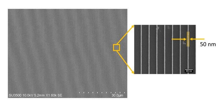
Demonstration of super-resolution lithography using 364 nm to expose commercial photoresist. The 50 nm linewidth is significantly below the traditional diffraction limit.
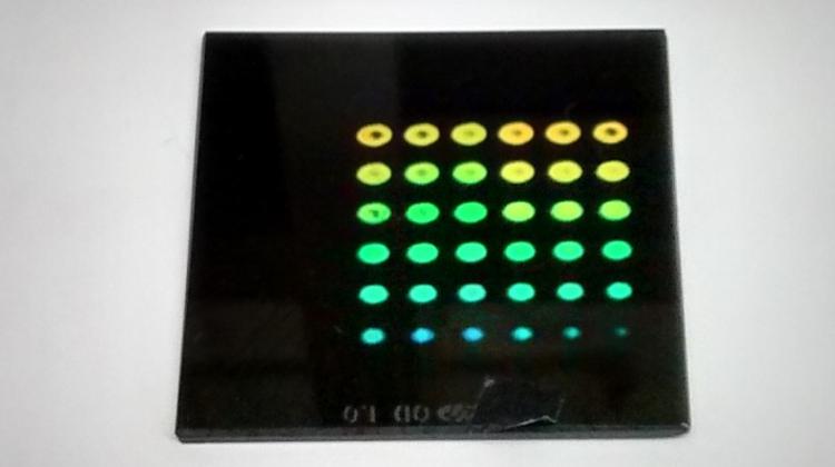
An array of interference lithography exposures testing response versus exposure time. The color is due to diffraction.
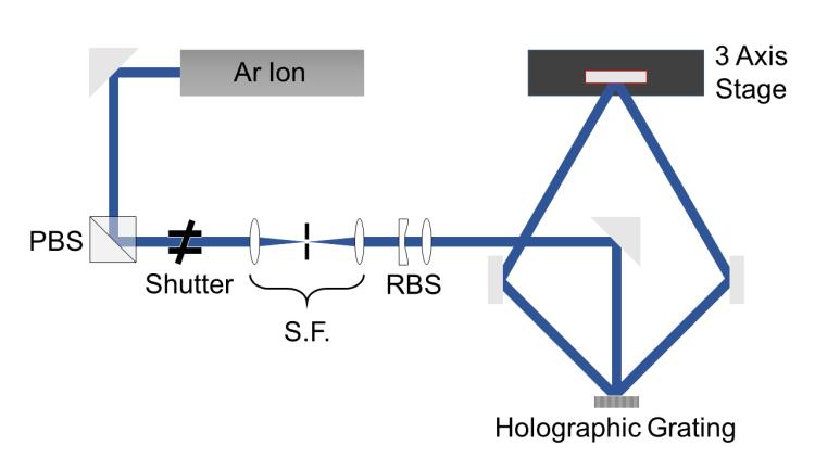
Layout of the interference lithography tool including a refractive beam shaper and holographic grating used as as beam splitter.
align="none"
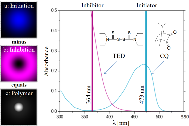
Our original material function. A diffraction-limited spot (a) at 473 nm creates initiating radicals via absorption by CQ. A Gauss-Laguerre "donut mode" (b) at 365 nm creates inhibiting radicals via absorption by TED. The resist polymerizes (c) only in the "donut hole" where initiation is not inhibited.