Method for Fabricating Corrugated Gate Dielectric-Semiconductor Interface Transistor

Background
Today’s trend in semiconductor chip manufacturing involves the miniaturizationof transistors and increasing the density of transistors per integrated circuit. Researchers at CU Boulder have developed a corrugated gate dielectric-semiconductor interface that can be easily incorporated into the existing semiconductor manufacturing technology to improve the transistor device performance.
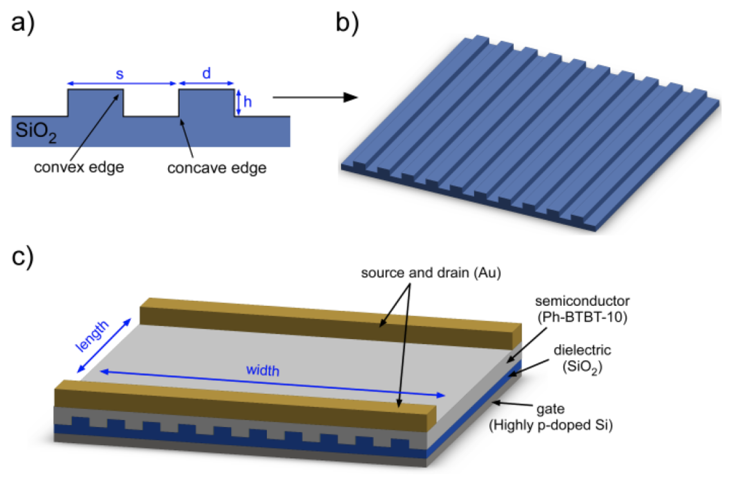
Fig. 1. a) Cross-section and b) three-dimensional view of the corrugated gate dielectric structure. c) A corrugated gate dielectric thin film field effect transistor with highly p-doped Si as the gate, SiO2 as the gate dielectric, Ph-BTBT-10 as the semiconductor, and Au source and drain electrodes.
Technology
The invention involves the introduction of micrometer-or nanometer-scale corrugations on the gate dielectric of transistors, particularly thin film field-effect transistors. We call this device a corrugated gate dielectric-semiconductor interface transistor. The corrugations can be patterned using semiconductor processing techniques, such as ultraviolet (UV) photolithography, electron beam lithography or nanoimprint lithography. The patterns are subsequently etched using reactive ion etching (RIE) and atomic layer etching (ALE) to produce the final corrugated gate dielectric layer. The presence of corrugations that run parallel to the length of the semiconductor channel from source to drain results in enhanced transistor device performance, specifically improvement in the “on” state drain current, higher on/off ratio and higher charge transport mobility compared to conventional planar gate dielectric transistors.
IP Status
Provisional Patent Filed
What's Next?
This technology is available for exclusive and non-exclusive licensing.
Nicole Forsberg: nicole.forsberg@colorado.edu
The Newsroom
For marketing and communication inquiries or news tips, contact Daniel Leonard, senior marketing and communications specialist for Venture Partners at CU Boulder.
For media inquiries, please visit colorado.edu/news/formedia.


