
Research
Current Research
Rugged and Efficient RF Wireless Power Receivers for Energy on Demand
Graduate researchers: Jack Molles, Allie Montgomery
Funded by: OECIF
Microwave rectification refers to the conversion of microwave power to DC power using a nonlinear element such as a diode or transistor. Rectennas integrate antenna elements with nonlinear elements to receive and rectify RF or microwave energy received from free space. There are two main uses for rectennas that can be applied over a wide range of RF and microwave frequencies:
1) Harvesting applications capture and rectify very low-power, ambient microwave energy. Harvesting is typically broadband in order to capture as much available energy as possible.
2) Power beaming applications receive anywhere from low-power (uW) to high-power (kW) directly beamed from one or more dedicated transmitters. Although broadband power beaming is possible, these applications tend to be much more narrowband than harvesting applications.
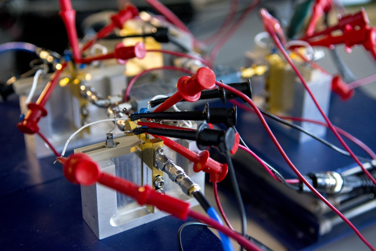
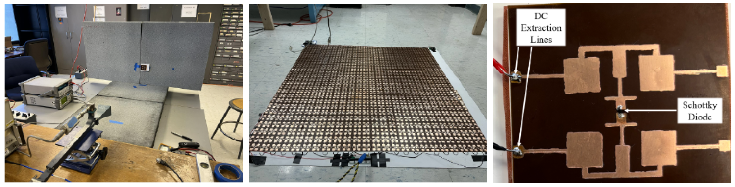
This project, funded by OECIF, aims to design and manufacture low-cost, rugged, flexible, and scalable planar rectennas for use at 10 GHz. The purpose of this project is to develop a reliable and easily deployable rectenna array to receive power from an overhead drone-mounted transmitter in energy-denied environments. This would allow for on demand emergency power regardless of time of day, cloud coverage, or dust storms which would all inhibit the use of solar power. Our team's current approach uses microstrip patch antennas etched onto a thin and flexible polyimide substrate. These microstrip antennas are supported by a thicker layer of expanded PTFE backed by a copper fabric ground plane and integrated with Schottky diodes. The rectenna elements are designed to be modular such that they can be easily DC combined to form larger arrays for applications that require higher power levels and farther distances from the transmitter.
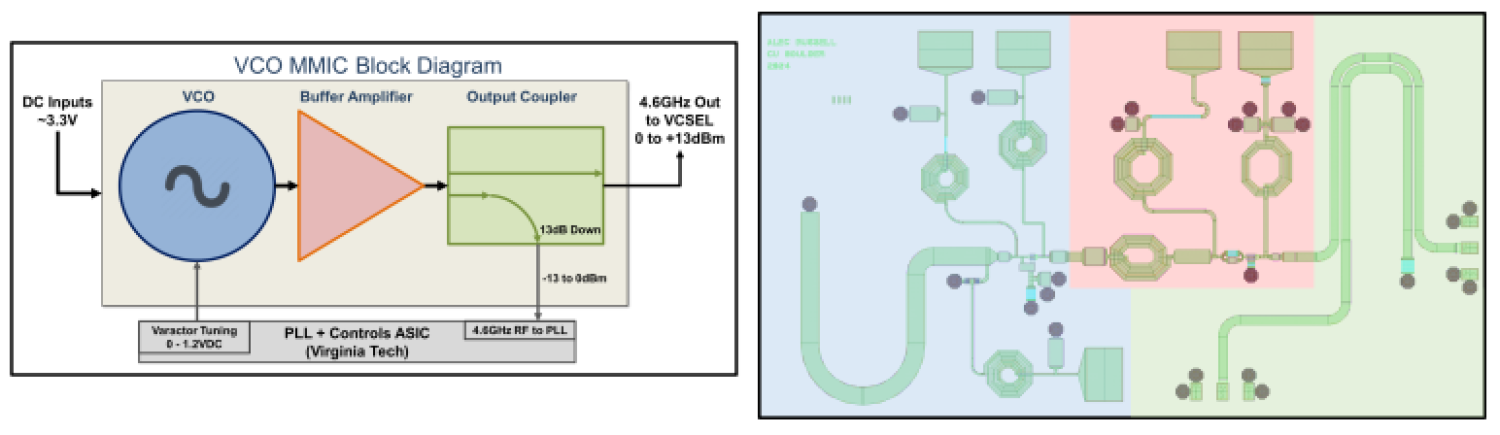
Low Phase Noise MMIC Oscillators for Chip-Scale Atomic Beam Clock
Graduate researchers: Alec Russell
Funded by: DARPA
The DARPA H6 program is a research initiative focused on creating new types of portable, low power consumption, long-term stable reference clocks. At CU Boulder we are focused on making a small, low-power, low phase noise, MMIC oscillator as a part of a new type of chip-scale atomic beam clock developed by NIST Boulder, with fabrication/packaging done by HRL, and control ASIC designed by Virginia Tech.
The operation of our team’s miniaturized atom beam clock is based on direct modulation of the current of a diode laser. These diode lasers are called vertical cavity surface emitting lasers (VCSELs) and are well suited to the design of ultra-miniature atomic clocks since low-power diode lasers can be modulated with low microwave power, and diodes with somewhat poor spectral purity can be used. When the VCSEL frequency is tuned (with current and/or temperature changes) to the optical resonant frequency (i.e. the D1 line of 87Rb) an increase in absorption is detected as a decrease in photodetector current. When the frequency of the VCO is simultaneously tuned to the hyperfine splitting frequency, an effect called coherent population trapping occurs. This results in an increase in light transmission through the atomic cell, observed as an increase in the dc current from a photodiode. Electronic feedback is then used to stabilize the VCO through a DC voltage on a varactor, which in turn creates an extremely stable frequency defined by the atoms that can be used as the output of the clock. This coherent population trapping scheme requires an oscillator that can be tuned to the hyperfine splitting frequency of the atoms within the atom beam, with low enough phase noise and power consumption such that the performance of the clock as a whole is not degraded.
Wearable Wireless Thermometers for Internal Body Temperature Measurements
Graduate researchers: Jooeun Lee, Sofia Mvokany, Henna Jethani, Joseph Dunbar
Funded by: The National Science Foundation
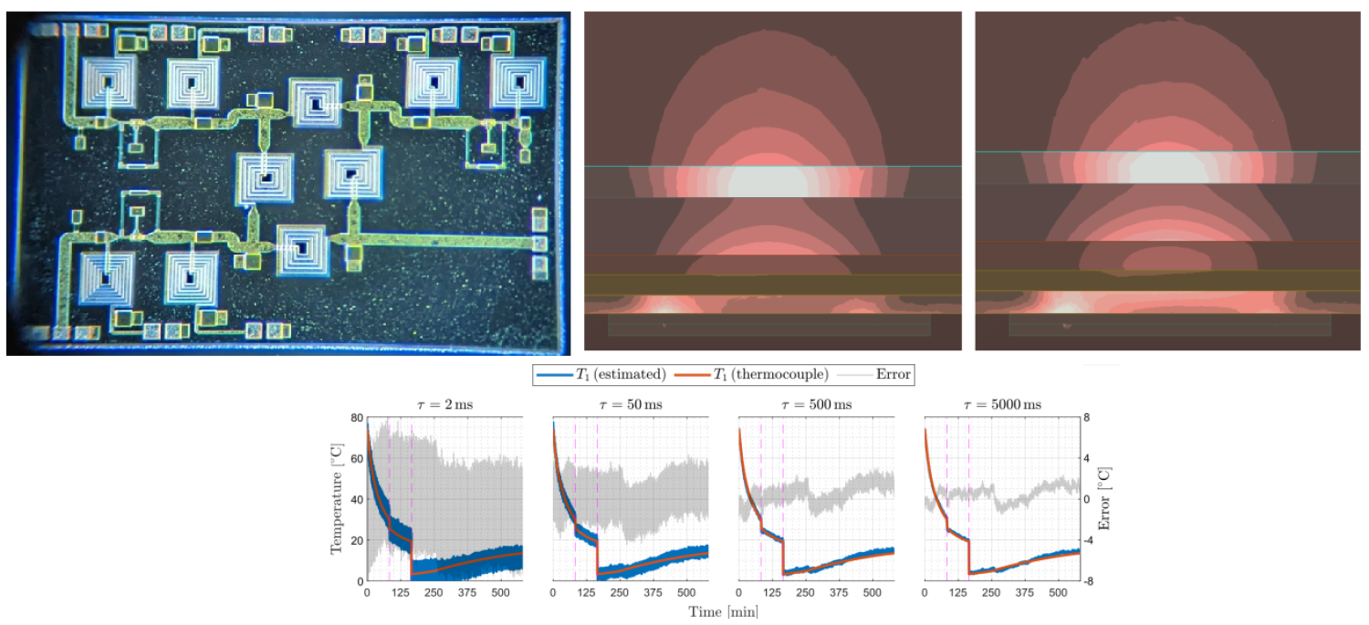
Microwave radiometry is an attractive method for internal thermometry, with the possibility of a wearable device which can continuously monitor temperature inside body tissues in different parts of the body, store the data, and transmit it to a digital medical record. Currently, there are a limited number of available device solutions, and they are usually not wearable or wireless. We are working on a possible path to implementing such a thermometer, with some initial results demonstrating about 0.2K measurement sensitivity and a difference between the maximal and minimal error w.r.t. a thermocouple measurement of 0.5K. Several probes for multi-band radiometers have been developed at frequencies of 410MHz, 1.4, 2.7 and 4.9 GHz. The main challenges of RF interference, sensitivity, calibration, spatial resolution, miniaturization, and probe design are discussed. The power received from tissues layers by the near-field probe is coupled to a variety of radiometer circuits, including Dicke, correlation, and other novel topologies. Controllable reference loads are used for continuous temperature calibration of the radiometer. The detector output is a DC voltage which can be integrated over time to increase the signal-to-noise ratio (SNR). This output is digitized, processed, and can be transmitted through a wireless unit.
In a number of disorders, core temperature changes are crucial and are not easy to measure externally. For example, long duration exercise in hot conditions, such as in the case of athletes, soldiers, or first responders, can provoke brain heating leading to premature fatigue and even death. Cancer cells can have increased temperatures, as can inflamed tissues such as joints of arthritis patients. Sleeping disorders are accompanied by changes in the circadian cycle, which are in turn related to changes in phase and amplitude of periodic core body temperature variations. Infants suffering from hypoxia-ischemia have an elevated brain temperature, which, if detected, can be effectively treated by hypothermic neural rescue. In addition to diagnostics, therapy can be assisted by internal temperature monitoring, e.g. in hyperthermia for cancer treatment and clinical high-intensity focused ultrasound (HIFU) for noninvasive therapy, where the knowledge of local temperature change would be useful.
Rydberg Atom Microwave Receivers
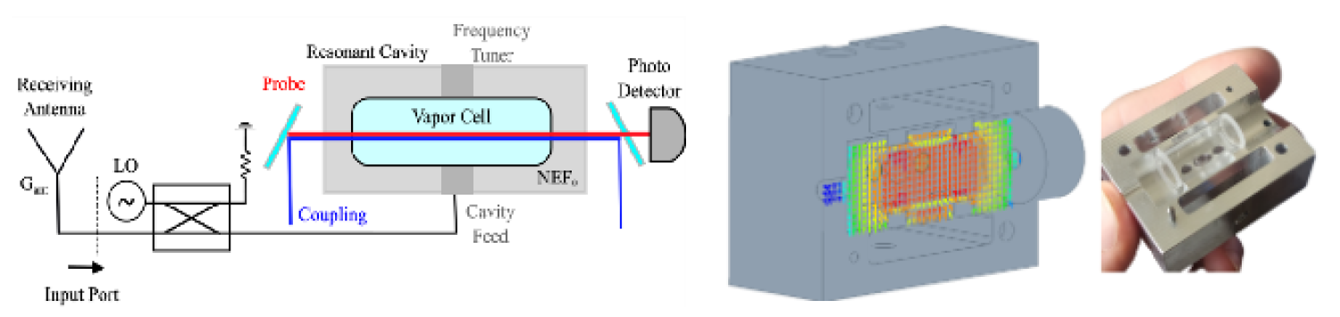
Graduate Researchers: Georgia Sandidge
Funded by: DARPA, Lockheed Martin
Atoms can be excited to Rydberg (high principal quantum number) states using standard lasers, so that their optical absorption characteristics become extremely responsive to the presence of RF electric fields. This effect can be leveraged to substitute the antenna and subsequent receiver frontend of a conventional receiver by a vapor cell illuminated by properly tuned and locked lasers. The resulting device is an RF field sensor/receiver with remarkable sensitivity, having the potential to approach the quantum limit. Furthermore, frequencies ranging from MHz to THz can be received using essentially the same device.
The microwave and RF research group is developing theoretical models that allow for a fair comparison between atom-enabled receivers and conventional frontends (such as e.g., LNAs and mixers) at microwave, millimeter-wave, and THz frequencies. Optimization of the experimental parameters involved in a Rydberg electrometry experiment is only possible through a comprehensive theoretical framework that relates atomic physics to engineering metrics, such as noise figure, dynamic range, instantaneous bandwidth, etc. We are currently engineering electromagnetic structures that enhance the field sensed by the excited atoms (e.g., high-Q resonant cavities), while minimizing thermal noise.
Millimeter-wave Front End Integrated Circuits
Graduate Researchers: Stefan Stroessner
Funded By: Air Force Research Laboratory, HRL Laboratory, WIN Semiconductor
Millimeter-wave frequencies are characterized by high-data throughput (from high bandwidth space), high imaging resolution (from small wavelengths), and penetrability through certain environmental conditions (e.g. atmospheric absorption windows as well as through dust, smoke, and fog). With growing user demand for extensive multimedia content with large storage and transfer needs, communication links are under development for current telecommunication systems in 5G lower mm-wave bands. Additionally, mm-wave communications are attractive for fixed satellite services and space exploration missions. The V-band, 50-75 GHz, and W-band, 75-110 GHz, is occupied with backhaul communication links for earth and space systems, mm-wave imaging, spectroscopy, radioastronomy, and automotive radar. In already developed high throughput geostationary multimedia services at K-band, W-band carrier frequencies could reduce the number of pathways for data transmission allowing allocated resources to reroute during failures. In deep space, the high directivity of high-element count compact antenna arrays in W-band is of interest. The drawbacks of using the frequencies in the mm-wave bands is high attenuation due to the tropospheric events and atmospheric phenomena. Due to high propagation loss, these applications can benefit from higher transmitted power levels (>1W); however, solid-state power amplifiers (PAs) are limited in total output power, bandwidth, and efficiency at mm-wave frequencies, requiring power combining and increased number of RF components in the analog front-end.
The microwave and RF research group has focused years on developing new MMIC topologies for millimeter wave circuits. Some past and present projects include Ka-band power amplifiers designed for high efficiency and high power through supply modulation and harmonic termination, and various W-band circuits, including power amplifiers, low noise amplifiers, phase shifters, switches, frequency multipliers, oscillators, and mixers, among others. Future MMIC runs through HRL Labs, Qorvo, and WIN Semiconductor provide opportunities to explore novel and established circuit topologies in emerging semiconductor technologies.
Transmit / Receive Modules for Advanced Phase Array Systems (TAPAS)
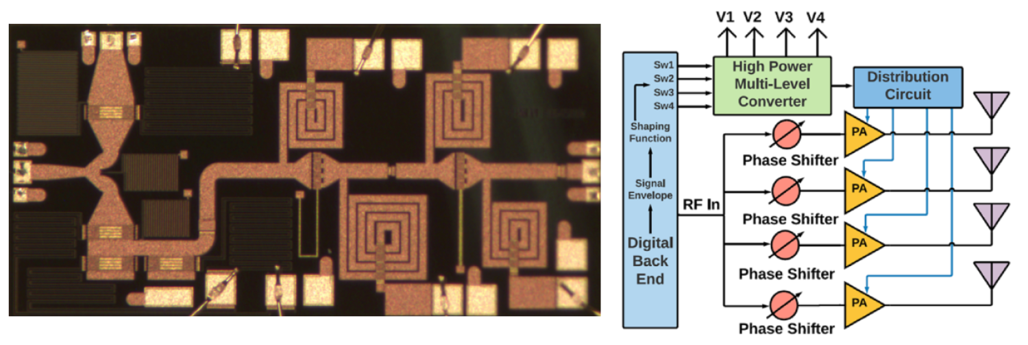
Graduate Researchers: Seth Johannes
Funded by: MIT Lincoln Laboratory
Transmit-receive (TR) phased arrays can operate in half or full duplex modes. When transmitting in half duplex, as done in pulsed radar systems, a switch is used to route the signal from the power amplifier (PA) to the antenna, reducing the available receive-mode time. Alternatively, a diplexer can be used between the antenna and TR module where the array transmits in an up-link frequency band, which is either closer or farther separated from the receive down-link band. In this case, the spectrum is not used efficiently and the diplexer can be relatively large and expensive, e.g. in cell phone base stations. Full duplex, or simultaneous transmit and receive arrays, usually require circulators, which are bulky, lossy and limited in bandwidth. Additionally, circulators have limited isolation which can be degraded when the impedance of the antenna changes during scanning. Our approach uses a fraction of the array elements for transmitting, while the remaining elements receive. This digitally-scanned array architecture is reconfigurable in terms of number of transmit and receive elements.
For an in-band full-duplex phased array, a limiting factor is the isolation between the transmitter and receiver paths. A part of the transmit power may leak into the receiver and saturate the LNA, or the analog-to-digital converter (ADC) in the downconversion path. This can be improved with self-interference cancellation (SIC) techniques, which can be implemented in the propagation domain, analog domain, or/and the digital domain. Focusing on an integrated GaN on SiC front-end, to allow for switching between transmit and receive for each element, along with sampling of the transmitted signal. A SIC technique can be implemented in the digital domain which compares the sampled transmit and receive signals, allowing for an in-band full duplex phased array.
High Power Supply Modulation of Octave Bandwidth Power Amplifiers for Efficiency Enhancement
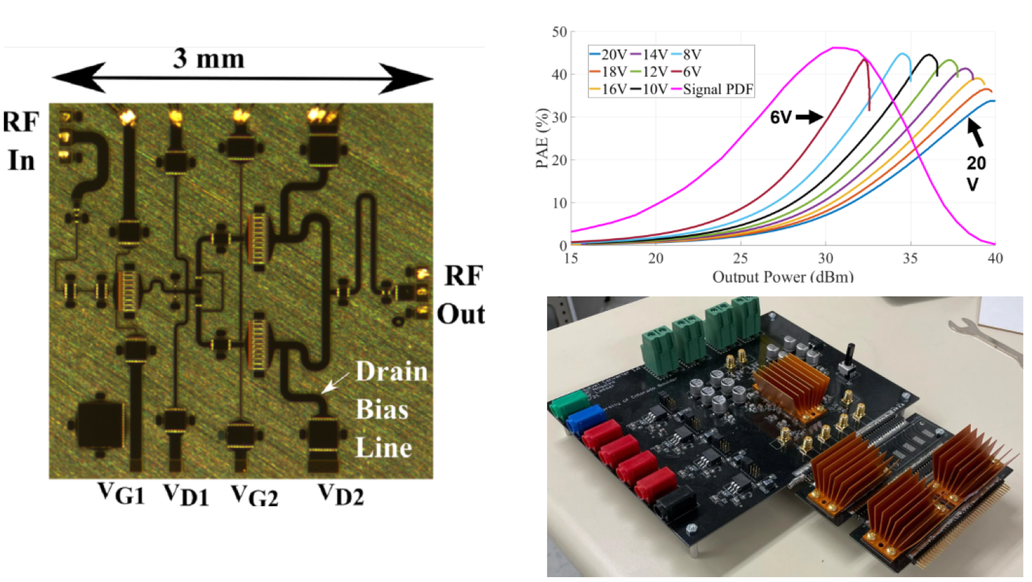
Graduate Researchers: Paul Flaten, Reyes Lucero
Funded by: Office of Naval Research
Modern RF and microwave systems demand broadband power amplifiers (PAs) that can amplify large signal bandwidths with high peak to average ratio (PAPR). Standard PA designs with static drain voltages suffer from low efficiency and degraded linearity when amplifying signals with high PAPR. One method to improve efficiency and linearity is through a technique called supply modulation where the drain bias of the PA is dynamically changed based upon the instantaneous power that the PA is amplifying. One major advantage of supply modulation is that it does not impose any RF bandwidth limitations on the PA design. The challenges of supply modulation include designing high speed power supplies with good efficiency and designing PAs that have high efficiency and low gain variation across different supply voltages. Continuous supply modulators, also known as envelope trackers, output a voltage that closely follows the signal envelope. A typical implementation of a continuous tracker is a buck converter. Unfortunately, buck converters must operate with a switching frequency that is at least an order of magnitude above the signal bandwidth in order to properly track the signal. This substantially degrades the efficiency of the supply modulator and overall system when utilizing signals with a high bandwidth. An alternative to continuous supply modulation is discrete supply modulation (DSM) where the output voltage is switched between some preset number of voltage levels typically using transistor switches. The advantage of DSM is it significantly reduces the number of switching instances and improves the supply modulator efficiency.
The Microwave and RF research group has designed several 6-12 GHz MMIC PAs in WIN semiconductor’s NP15 GaN on SiC process. In addition, this group works on the design of high-power DSMs capable of supplying a peak output power of 1KW at 20V with a switching speed of 10 MHz. The high-power DSM can be used to supply a phased array system consisting of many PA elements or a single high power PA.
Past Projects
GaN-On-Si Chip Process Development
Graduate researcher: Philip Zurek
In partnership with Lincoln Laboratory, we are investigating a new GaN-on-Si process that demonstrates the capability of using silicon as a substrate for gallium nitride-based power amplifiers instead of the more frequently found silicon carbide. Silicon is a promising substrate for decreasing cost and size and enabling single-chip integration with CMOS technologies. Thus farm electromagnetic properties of the GaN-on-Si chip have been simulated to obtain accurate transmission-line and lumped component circuit models. GaN transistors are tested to develop several kinds of models to characterize their performance under conditions a PA may expect to operate under. Using this information, power and high-efficiency focused PAs may be designed and fabricated using the new process. Ultimately, these designs and fabricated circuits will be integrated with the CMOS processing necessary to develop a full transceiver-on-chip.
High Field MRI Probes
Graduate researcher: Patrick Bluem
In clinical 1.5 T and 3 T magnetic resonance imaging (MRI) instruments, the object being imaged is closely coupled to the detector through near fields and detection can be viewed as quasi-static. MRI can also be excited and detected using long-range coupling with traveling waves, demonstrated by several research groups over the past few years. One potential benefit of this approach is more uniform coverage of samples that are larger than the wavelength of the NMR signal. Uniform spatial coverage in MRI is traditionally achieved by tailoring the reactive near field of resonant probes. This approach is valid when the radio-frequency wavelength at the Larmor frequency is substantially larger than the target volume, which does not hold for wide-bore high-field systems (>4 T and >60 cm bore diameter). The motivation for using high DC magnetic flux density (B0 > 3 T) is increased spatial resolution, improved SNR, better parallel imaging performance and potential for improved contrast. However, the proton Larmor frequency for hydrogen increases from 64 MHz at 1.5 T to 447 MHz at 10.5 T, resulting in waveguide effects both in the bore and the imaging volume. To help control the excited modes, structures are placed around the imaging volume to modify the boundary conditions.
In collaboration with Harvard University and the Center for Magnetic Resonance Research (University of Minnesota), circular patch probes have been measured on 16.4 T small-bore, 7 T wide-bore, and 10.5 T wide-bore scanners.
Package Design for Improving Active Device Efficiency
Funded by: Infineon
Graduate researcher: Sushia Rahimizadeh
Active devices, such as transistors and diodes, are often packaged to allow easier integration with circuit boards. At RF and microwave frequencies, the reactances of the package limit the impedance range that can be presented to the intrinsic device. Additionally, this parasitic reactance is largely capacitive and will limit the harmonic content necessary for achieving high-efficiency operation. In cooperation with Infineon Technologies, packages are designed to present desirable harmonic impedances to the device by using a combination of bond-wires, MOS capacitors, and package parasitics. Accurate full-wave modeling of the passive package environment is demonstrated along with a methodology for manipulating package and bond-wire geometry to achieve specific harmonic impedances. The package model is used in conjunction with harmonic balance simulations including a transistor die non-linear model to design harmonically-terminated packages for highly-efficient power amplifiers at S-band.
LabVIEW Open LSNA Toolbox
Funded by: National Instruments, CU Boulder
Developed by: Dr. Tibault Reveyrand
This LabVIEW toolbox enables high level functions on your current instrumentation while presenting high-level abstraction. After defining basic drivers of your instrumentation, the user can conect to power meters, load-pull systems, vectorial receivers and even several calibrated LSNAs with just one polymorphic VI. The toolbox comes with several examples in LabVIEW. One of them is a complete DC power supply sweep and S-parameters measurements dedicated to transistor measurements.
The Large Signal Network Analyzer is an already defined meta-instrument in the toolbox and includes its own calibration procedure. An LSNA can be built without any downconverter, with mixers or sub-samplers.
The theory behind the LabVIEW code was covered in a Special Topics course taught by Dr. Reveyrand in spring 2016. A version of the toolbox (with proprietary external software removed) is available for download.