
Carrier transport in heterojunction nanocrystals under strain
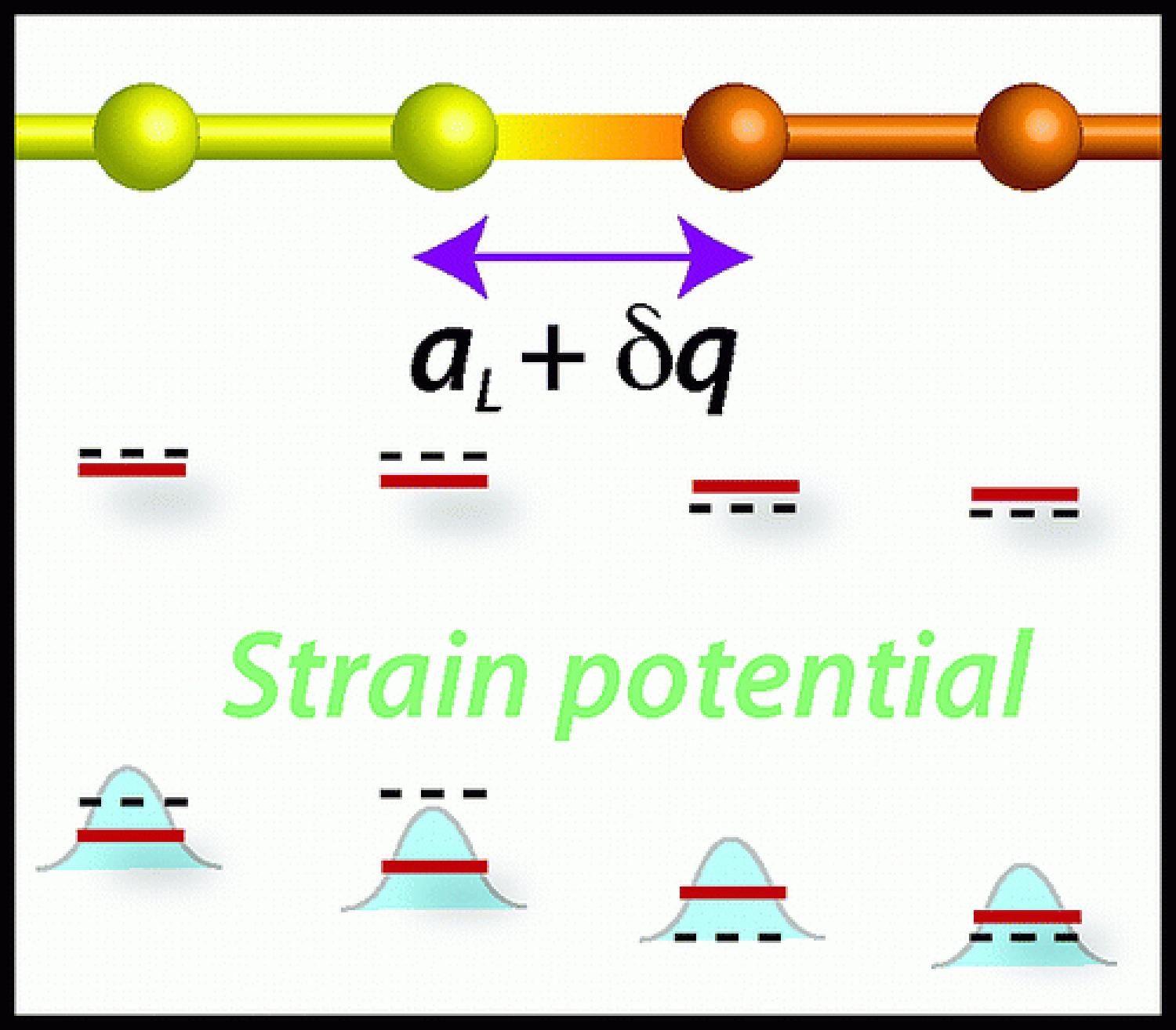
We present a theory for carrier transport in semiconducting nanoscale heterostructures that emphasizes the effects of strain at the interface between two different crystal structures. An exactly solvable model shows that the interface region, or junction, acts as a scattering potential that facilitates charge separation. As a case study, we model a type-II CdS/ZnSe heterostructure. After advancing a theory similar to that employed in model molecular conductance calculations, we calculate the electron and hole photocurrents and conductances, including nonlinear effects, through the junction at steady state.
Sweeney, M. C. and Eaves, J. D. Carrier transport in heterojunction nanocrystals under strain. J. Phys. Chem. Lett. 3, 791 (2012)
Categories: 2012